Next: Introduction, Up: (dir) [Contents]
This document is a manual for PCB, the interactive printed circuit board layout system.
| • Introduction: | Introduction to PCB | |
| • Terminology: | Terms and definitions. | |
| • Installation: | ||
| • Your First Board: |
Next: Terminology, Previous: Top, Up: Top [Contents]
PCB includes a stand-alone program (called pcb) which allows
users to create, edit, and process layouts for printed circuit boards,
as well as a library of footprint definitions for commonly needed
elements. While originally written for the Atari, and later rewritten
for Unix-like environments, it has been ported to other operating
systems, such as Linux, MacOS/X, and Windows.
While PCB can be used on its own, by adding elements and traces
manually, it works best in conjunction with a schematic editor such as
gschem from the gEDA project, as gschem will create a
netlist, make sure all the elements are correct, etc.
The file in which pcb stores its data ends in .pcb such
as myboard.pcb. Additionally, pcb reads individual
element footprints from files ending in .fp and netlists from
files ending in .net.
There are a couple of different outputs from pcb. If you are
having your boards professionally fabricated, you will want to export
your board as an RS-247X (aka gerber) file. If you are fabricating
your board yourself, you’ll probably want to print it. You can also
save it as an encapsulated postscript or image file for use in
documentation and/or web pages.
A note about typography: Throughout this document, “PCB” refers
to the whole package, “pcb” refers to that specific program,
and “pcb” refers to a generic printed circuit board.
Next: Installation, Previous: Introduction, Up: Top [Contents]
There is some variation in terminology used by EDA packages. To best understand the PCB documentation, it’s important to read through these definitions so you understand how PCB uses these terms.
Internally, most pcb commands use a common interface to connect
to the GUI, scripts, and user requests. We call these internal
commands actions, because they are actions that pcb can take. Each
action may take parameters, according to their individual
documentation. Actions are written like function calls, and may be
invoked directly from within PCB using the ’:’ key.
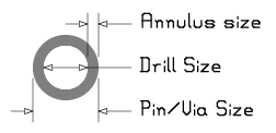
The donut-shaped ring of copper that surrounds the hole of a pin or via. In PCB, the size of a pin or via is the overall diameter of the copper, not the distance from the outer edge of the hole to the outer edge of the copper. When we refer specifically to the size of the annulus, we mean the distance from the hole’s outer edge to the copper’s outer edge; i.e. the amount of copper remaining around a drilled hole. Example: a 30 mil drilled hole with a 8 mil annulus results in a 46 mil pin (30 + 8 + 8). Likewise, a 50 mil pin with a 30 mil drill results in a 10 mil annulus.
In reference to RS-274X files, an aperture is a brush shape used to draw things. Originally, the aperture was a physical hole of a specific shape and size through which light exposed a photographic film.
A curved trace drawn on a drawing layer.
Varied meanings. Elements and boards
may have attributes assigned to them, which are arbitrary mappings
between a name and its value. PCB does not currently use those
attributes itself. Within pcb an attribute is an arbitrary
value passed between the core and the various HIDs, such
as checkboxes and file names.
The most that the copper areas can be expanded before they are allowed to touch. For example, two 40 mil lines 10 mil apart can bloat up to (but not including) 5 mil before they touch, so the maximum bloat would be 4.99 mil.
The physical printed circuit board that is depicted by your layout. “Board” refers to the physical board, “layout” refers to the electronic data.
A temporary storage location within pcb where items can be
stored until needed later. One such buffer is used for the common
cut-and-paste operations.
A thin layer of copper attached to a thin layer of insulator. Once etched, the remaining copper forms the electrical connections described by the layout file.
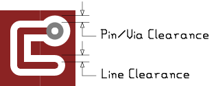
The distance beween the copper around a hole (the annulus) and the copper in the surrounding polygon, or between any other copper item (line or arc) and a surrounding polygon.
The area around an element which is still “used” by the element, for its electrical and mechanical clearance requirements. PCB does not use this term, nor explicitly support a courtyard definition for elements.
This is the actual location on the board which is used when you perform an action. If grid snap is active, the crosshair reflects the grid point closest to the cursor, else the crosshair reflects the cursor itself.
PCB is referring to your mouse cursor. See “crosshair”.
While designing your circuit board, PCB provides a number of layers to draw on. While it’s convenient to think of each drawing layer as corresponding to one of the physical layers (copper, silk, etc), it’s possible to group multiple drawing layers together into one physical layer, or assign drawing layers to purposes not corresponding to physical layers. For example, you could have two drawing layers corresponding to your ground plane copper layer, one for the ground plane itself and a second (differently colored) one for any signals that need to be routed on the ground plane layer.
Design Rule Check. Your design is scanned and compared to a number of design rules, such as minimum trace thickness and spacing, and any violations are noted. Then, you are tortured to death with non-modal dialogs.
A computer-readable file intended to be used by automated drilling
machines. The information includes drill diameters and locations.
pcb may produce up to two drill files, one for plated
holes and one for unplated holes.
Automated drill machines were originally designed by the Excellon
company, so drill files are sometimes called excellon
files. Also called an NC drill file.
In PCB an element represents any part you might install on your board, such as resistors, capacitors, and integrated circuits. Note that this also includes anything on your board that has its own footprint, even if it doesn’t have a part associated with it, such as test points, registration targets, and edge connectors. An element has a footprint, but is more than a footprint - it also has a reference designator (refdes), value, description, and location. “Footprint” refers to the pattern; “element” refers to the instance. For example, your layout might have four elements that use one footprint.
Not to be confused with solder resist, etch resist is used during the fabrication of the copper layers to define what copper is removed and what copper will remain.
See drill file.
A company that produces (fabricates) circuit boards from mechanical design files. Most accept (or expect) gerber (RS-274X) format files.
A drawing that shows a mechanical overview of the board, including the physical outline and all physical holes. This is often used by fabs to sanity check their interpretation of your design files.
A footprint is the pattern on a circuit board to which your parts are attached. This includes all copper, silk, solder mask, and paste information. In other EDA programs, this may be referred to as a “land pattern”. “Footprint” sometimes is used to refer to a footprint file. “Footprint” refers to the pattern; “element” refers to the instance. For example, your layout might have four elements that use one footprint.
A file that contains a single footprint definition. Normally, this means it describes one element, although there are exceptions.
A specification for the insulating layer used in printed circuit board manufacture. FR4 is the most common grade, and is often an epoxy fiberglass composite.
The GPL’d Electronic Design Automation suite of tools. See
http://www.geda.seul.org. It includes, among other things, the
gschem schematic editor, which produces input that pcb
can use.
The common name for an RS-274X formatted file. Originally named after the Gerber Photoplotter Company.
A pattern of locations on the board which can be displayed, or used as a limit on crosshair locations.
The schematic editor that comes with gEDA.
Human Interface Device. We use this term to refer to user interfaces,
printers, exporters, and other ways that pcb interacts with
humans.
A region created by the designer solely to prevent something else from existing there. For example, an element with a copper keepout would prevent the autorouter from routing traces through that area. PCB does not currently support keepouts.
There are two meanings of “layer” in PCB. See “drawing layer” and “physical layer”.
The board design information depicted by the edits you’ve made; this is what’s stored in a pcb file and displayed on the screen. “Board” refers to the physical board, “layout” refers to the electronic data.
A straight segment drawn on a drawing layer.
Normally, pcb reports coordinates relative to the origin (upper
left) of the board. However, you can designate a location on the
board such that pcb also reports coordinates relative to
that location. Such a location is the mark, and is drawn with an X
shape. Elements also have a mark; this is the local
origin from which other locations within the element are
measured. Element marks are drawn as small diamonds.

See “solder mask”.
In PCB a mil is 0.001 inch, or a “milli-inch”. Other packages may call it a “thou”, short for a thousandth of an inch.
Numerically Controlled Drill file. See “drill file”.
For most drawing layers, the stuff you draw
corresponds to stuff that exists in a physical layer. For
example, a trace drawn on a copper layer results in copper
existing on the board. For negative layers, however, what you
draw results in what does not exist on the board. The
solder mask gerber, for example, is such a layer - a
circle drawn in the solder mask gerber results in a hole in the
physical solder mask. pcb represents such layers in a
meaningful way on the screen, but exporters may use a negative layer
according to the needs of the fabrication process.
A list of symbolic electrical connections, normally provided as input
to pcb from a schematic layout program, which represents the
desired electrical connectivity of the board. PCB can compare the
desired (loaded) netlist with the actual (copper) netlist and advise
you of shorts or unrouted connections. If there are unrouted
connections, it can use those to create a rat’s nest to assist
you in routing them.
The physical shape and dimension of your physical board. By default, this is a rectangle the size of your working area (the “board size”), but if you name one of the drawing layers “outline” that is used instead. While your board is itself a polygon shape, a polygon drawing object is not used to denote its outline - by convention, 10 mil wide lines are used to draw the outline, and the centerlines of those lines indicate the actual outline edges.
An electrical connection to an element which does not require a through hole, for example as used by a surface mounted device.

See “solder paste”.
A thin sheet, usually plastic or metal and 0.002 to 0.005 inches thick, with holes where solder paste should be applied to your board.
A file used by pcb to store board layout. Such files end in
.pcb and are normally readable (and editable) text files.
Internally, pcb maintains all measurements in its own units,
which are smaller than both mils and millimeters. These are the
default units used in PCB files. At the time this text was written,
pcb units are 1/100 of a mil, or
10-5inches.
An electrical connection to an element which requires a through hole, for example as needed by a DIP socket. Contrast with a pad. Note that pins and vias are mechanically identical, although pins default to untented while vias default to tented.

In the manufacture of circuit boards, a physical layer is, for
example, each layer of copper, each side’s silkscreen, the
solder mask, the paste stencil, the physical outline,
etc. Each physical layer requires a single layer definition to be
produced by pcb; for professional fabs there is one
gerber file for each physical layer.
During fabrication, some holes become coated with copper which connects all the copper layers together at that point. Since this is normally done by electroplating, such holes are called “plated” holes, and normally have a copper annulus around them.

A polygon defines the ouline of a drawn region on a drawing layer. When used on a drawing layer representing a copper physical layer, it causes a copper polygon to exist in the final board, for example. Unlike lines and arcs, a polygon does not have a “thickness” as the lines define the exact boundary of the shape.
A rat is a symbolic visual representation of an unconnected electrical
connection - i.e. something in the netlist which doesn’t exist
as a trace yet. It’s called a rat’s nest because of its messy
appearance when first created, from that, the individual connections
were named rat lines or just rats. In a PCB file, the rat list is
a list of all rats that exist on the board; this isn’t always the same
as the netlist, because you may choose to work with a subset of
the netlist at a time, or hide the rats completely. Many
pcb functions use a rat list to determine which connections to
work with; it is important to update the rats list before using such
functions.
A special case of polygon.
In PCB this usually means the etch resist.
In PCB this term is a verb, meaning to add and arrange traces so as to properly reflect the netlist. Other packages may use this term to reflect the outline, but PCB does not.
A collection of sizes, such as trace thickness, drill diameter, pin size, and clearance, which is used when routing traces. PCB can keep track of at least four styles, which you can quickly switch between.
A file format used originally by photoplotters, but now used by any machine used to fabricate circuit boards. The D variant requires a separate file defining all the apertures, and is considered obsolete. The X variant is newer and includes the aperture definitions, and an X2 variant is now available that includes embedded attributes. Since these formats were defined by the Gerber Photoplotter company, they are commonly known as “gerber files”. The RS-274 family of specifications is currently owned and developed by Ucamco and are available at http://www.ucamco.com/downloads.
The most that a copper area can decrease in size before it no longer touches (overlaps) an adjacent copper area.
A layer of ink or pigment drawn on the circuit board (usually, one for each side of the board) in order to include, for example, part numbers or element outlines.
A layer of heat resistant film placed over the outermost copper layers
of your board, to prevent solder from sticking to any covered copper.
When used to cover traces routed between
pins or pads, this can help avoid shorts to
those traces. Note that when shown in pcb the
mask is drawn where the film exists, but when output (to postscript or
gerber, for example), it is often “drawn” where the mask is
to be removed.
See solder mask.
Ground up solder mixed with flux. This paste is normally squeegeed through a paste stencil to deposit a measured amount of paste on each pad on the board. Once the paste is applied, parts can be positioned on the paste, and the board heated - which melts the paste and solders the parts to the board.
When a circuit board is made with a solder mask, you have the option of opening a hole in the mask over vias, or leaving the mask intact over them. A via with an intact mask over it is tented, as the mask acts like a tent over the copper and hole.

Since copper is an efficient heat sink, connections to a large region of copper would be very difficult to solder - the copper heat sink prevents you from adequately heating the connection. To fix this, small cutouts are made around each such connection to create a thermal barrier, so that heat applied to the connection stays at the connection. Such a set of cutouts, and the copper bridges that remain, is called a “thermal”. Thermals come in many patterns, which allows the designer to ensure adequate electrical connectivity and/or manufacturability.

In PCB this often refers to the width of a line or arc, not the thickness of the copper film used to produce the board. This is also the “size” of a line or arc.

A mode used by pcb’s GUI by which board objects are drawn as
thin lines (or outlines) rather than as actual-width lines. This mode
is useful for detail work where the size of the objects would
otherwise obscure their relationship to each other.
See “mil”.
A home-fabrication method that involves printing a layer with a laser printer, and transferring the toner from that print to an unetched copper board. The toner acts as an etch resist.
Any copper added to a copper layer whose purpose is to connect electrical signals between elements. Traces may be built up from lines, arcs, and polygons.
During fabrication, some holes are drilled after electroplating, and so do not receive the copper that would otherwise connect layers. Such holes are unplated holes, and normally do not have a copper annulus around them either.
When a hole is placed in the solder mask in order to expose a via below it, such a via is untented. Untented vias are available as test points or places to add wires later.
A via is a connection between different copper layers. In PCB all vias are “through” vias, in that they connect copper on all layers.
Next: Your First Board, Previous: Terminology, Up: Top [Contents]
| • Installing a Pre-Built Package: | ||
| • Building From the Source CD: | ||
| • Building From CVS: |
Next: Building From the Source CD, Up: Installation [Contents]
| • Debian: | ||
| • Fedora: | ||
| • Gentoo: | ||
| • NetBSD: | ||
| • Ubuntu: |
Next: Fedora, Up: Installing a Pre-Built Package [Contents]
apt-get install pcb
Next: Gentoo, Previous: Debian, Up: Installing a Pre-Built Package [Contents]
To automatically download and install the latest version (and dependencies) from one of the (pre-configured) Fedora repositories:
yum install pcb
For the installation with yum you need administrator-privileges.
To install a manually downloaded rpm:
yum localinstall <rpmfilename>
Where <rpmfilename> is the downloaded rpm of your choice. Required dependencies need to be downloaded and installed simultaneously, or beforehand.
"localinstall" is used to install a set of local rpm files. If required the enabled repositories will be used to resolve dependencies. Note that the install command will do a local install, if given a filename. This option is maintained for legacy reasons only.
"localupdate" is used to update the system by specifying local rpm files. Only the specified rpm files of which an older version is already installed will be installed, the remaining specified packages will be ignored. If required the enabled repositories will be used to resolve dependencies. Note that the update command will do a local update, if given a filename. This option is maintained for legacy reasons only.
Next: NetBSD, Previous: Fedora, Up: Installing a Pre-Built Package [Contents]
emerge pcb
Next: Ubuntu, Previous: Gentoo, Up: Installing a Pre-Built Package [Contents]
See ftp://ftp.netbsd.org/pub/NetBSD/packages/pkgsrc/cad/pcb/README.html.
Previous: NetBSD, Up: Installing a Pre-Built Package [Contents]
Next: Building From CVS, Previous: Installing a Pre-Built Package, Up: Installation [Contents]
Previous: Building From the Source CD, Up: Installation [Contents]
| • Unix/Linux: | ||
| • Mac OS/X: | ||
| • Cygwin: |
Next: Mac OS/X, Up: Building From CVS [Contents]
Next: Cygwin, Previous: Unix/Linux, Up: Building From CVS [Contents]
Previous: Mac OS/X, Up: Building From CVS [Contents]
Previous: Installation, Up: Top [Contents]
In this chapter, we’re going to walk you through creating a few very simple boards, just to give you an idea of the way the programs work and how to do the things that are common to all project. Each board will build upon techniques learned from the previous board.
While this manual is not intended to cover the gschem program,
we will be instructing you on the minimum you’ll need to know to use
gschem with pcb. Please refer to the gschem
documentation for further details.
The first board will be a simple LED and resistor. It will show you how to create a board, place elements, and route traces. The second board will be a simple LED blinker, which will involve creating schematics, setting up a project, and creating new symbols and footprints. The third board will be another blinker, this time with surface mount devices and four layers, which will introduce power planes, vias, and thermals.
| • LED Board: | ||
| • Blinker Board: | ||
| • SMT Blinker: |
Next: Blinker Board, Up: Your First Board [Contents]
This first board will show you the basic operation of pcb.
Each new command or operation that is introduced will be described in
full the first time, but not subsequent times. Many operations can be
invoked either by a menu option, like File→Quit Program to
select the “Quit” option in the “File” menu, or by a keyboard
shortcut, like Ctrl-Q. When we say Ctrl-Q we mean to hold
the Ctrl key while pressing the Q key. When we say
Shift-Q we mean to hold either Shift key while pressing
the Q key.
For example, the first time we describe the Quit command, we’d say,
“now exit pcb by using the Quit command (File→Quit or
Ctrl-Q)”. Any other time, we’d just say “now Quit.”
The first step in this project is to run pcb. Since pcb
defaults to using the current directory for its files, it’s a good
idea to create a new subdirectory for this project, cd into it
in a terminal window, and then run pcb from there:


Now is a good time to practice that Quit command :-)
Also, if you ever ask for pcb help from someone else, they’ll
probably want to know what version and GUI you’re using. To see this,
use the About command (Window→About...).
Note that when pcb starts, it creates not only its main window
(pictured above), but two additional windows. One is the “PCB
Library”, which we’ll talk about later, and the other is the “PCB
Log” that contains all the messages - warnings, errors, etc. For
now, you can just move these out of the way. If you close these, you
can re-open them using Window→Library and Window→Message
Log.
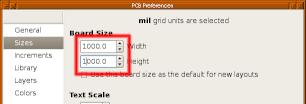
For any board you create, one of the first things you need to decide on is how big the board is going to be. If you want it to be “as small as possible”, then you can create it bigger than you need and change the size later. For this simple board, we can guess - we want it to be one inch by one inch. The board size controls are located in the Preferences window (File→Preferences), which contains both board-specific and user-specific preferences. We want the Sizes preferences, so click on the word Sizes. The window should look like this:
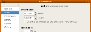
We won’t be using the Text Scale or DRC preferences yet. Note that
the units are mils, so the default board size is six inches wide and
five inches high. Change these numbers to 1000.0 each:
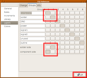
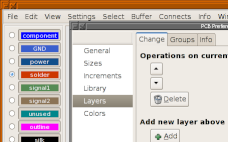
We will next set up our layers, which define how many copper layers we’ll have and what they’ll be called. Select the Layers preferences. You’ll see three tabs along the top; click on the Groups tab to show the layer group preferences. For this project, all we want to do is make sure that the solder layer is on the solder side, and the component layer is on the component side. Click in the boxes to make “component” and “component side” in group 1, and “solder” and “solder side” in group 2, then click on OK:
There’s a couple of settings you’ll want to set up now, as they get saved with the board. First, let’s turn on the grid (View→Enable visible grid if it isn’t already checked) and set it to 0.1" or 100 mil (View→Grid Size→100 mil). The grid is drawn as a field of tiny dots, which may be hard to see on our board but would be easier to see if there were more of them. For example, switch to a 10 mil grid and note the difference (don’t forget to switch back to 100 mil).
Next, we want to make sure any new traces we create won’t automatically connect with any polygons we might add - for example, adding a ground plane or “flood fill”. The Settings menu has many settings in it, but for now, just make sure that New lines, arcs clear polygons and Crosshair snaps to pins and pads are checked, and Auto enforce DRC clearance is not checked.
Now that we’ve set up our board, it’s a good time to save it. Use the
Save command (File→Save layout). Since this is the first time,
it will ask you for a layout name. We’re going to call this layout
fb-led.pcb so type that in where it says Name and click OK.
Now that your board has a file associated with it, you can just
File→Save layout whenever you want to save your work.
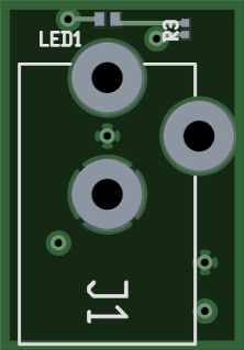
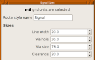
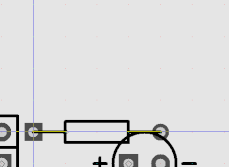
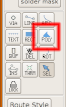
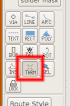
Now we’ll start adding the actual circuit. This circuit will be a simple LED in series with a resistor, and a header for a battery. We won’t need schematics, we’ll just add the parts and connections manually. The first step is to choose a route style for your new traces. The lower left corner lists the four available route styles. Make sure Signal is selected, then click Route Style to bring up the route style window. We’re going to use fairly large traces, which is typical of a simple board. In that window, set the Line width to 20, Via hole to 36, Via size of 76, and Clearance to 20; then click OK:

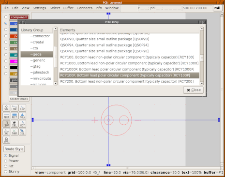
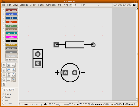
Next we’ll add the three parts we need. In larger projects, this will
be done by gsch2pcb but you’ll need to know the footprint names
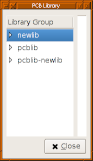
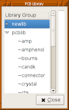
for that. Find the library window (if you left it open) or open it
(if you closed it) with Window→Library. Click on the triangle next
to pcblib to open the pcblib library. Scroll down to ~geda and
click on it, to open the ~geda library.
When you choose the parts out of the library, notice that there is
some text in square brackets - this is the footprint name you’ll need
for gsch2pcb. The first we want is the LED. We’ll use
RCY100P for the LED, which is a radial cylinder, polarized, 100
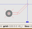
mil spacing. Scroll down until you find it, and click on it. When
you move the cursor back to the pcb window, you’ll see that it
now carries the outline of the part with it:
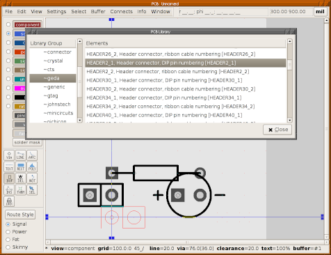
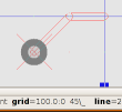
Press the left mouse button to place a part on your board. We’ll move
it later. Do the same for an ACY400 footprint for the
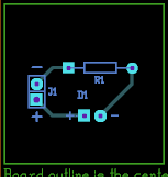
resistor, and a HEADER2_1. Your board should now look
something like this:
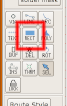
We will use the selection and rotate tools to position the parts where we want them. The palette of tools is just above the route styles, on the left. The two we want are SEL and ROT:
First click on the ROT (rotate) tool. The cursor should change shape to act as a hint that you’ll rotate whatever you click on. Position the cursor over the square pad on the header and click the left mouse button:
Now click on the SEL (selection) tool, also known as the “arrow tool”. You move parts by pressing the left mouse button while the cursor is over the part, and moving the mouse while holding the mouse button down. The part itself doesn’t move; instead, a wire-frame outline of the part is moved (much like when placing parts). When you release the mouse button, the part is moved.
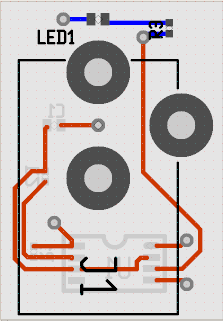
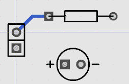
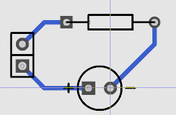
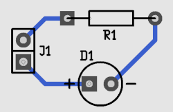
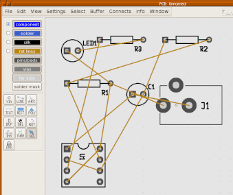
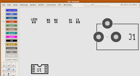
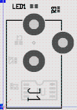
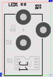
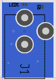
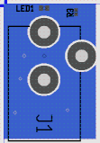
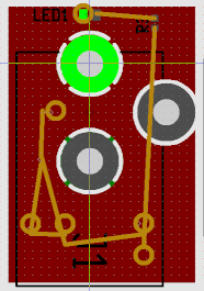
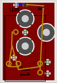
Move the header so that the square pin is at 200,600 (the crosshair’s coordinates are shown in the upper right corner of the window), the resistor’s square pin at 400,400, and the LED’s square pin at 500,700. Your board should now look like this:
Now is a really good time to save your layout.
Next we’ll start adding the traces that connect the parts. We’ll use the LINE tool to add them. Since this is a simple board, it’s likely to be built as a single-sided board, with the traces on the “back” side, so we want the solder layer to be the drawing layer. On the left side of the window is a collection of buttons named after various layers in your board. One of them is named solder. To the left of that button is a small indicator. Click on it. Don’t click on the button itself - that changes the visibility of the layer. Click on the indicator.

The way the line tool works is that you click on the starting point, move the crosshair to the end point, and click again. By not requiring you to hold the mouse button down, you have the ability to scroll and zoom to find the endpoint. You can also click on intermediate points to make lines with multiple corners. To end the trace, or start a new trace elsewhere, press the Esc key. If you press the Esc key again, you return to the selection tool.
If you attempt to connect two points that aren’t on the same vertical,
horizontal, or diagonal line, the line tool will create a pair of
traces to connect them. One will be either vertical or horizontal,
and the other will be diagonal. The vertical/horizontal segment will
be connected to the starting point, and the diagonal segment will
follow the crosshair. If you look in the status bar, you’ll see a
_/ symbol that indicates this:

Pressing the / key changes this mode. If it says \_ the
diagonal will attach to the starting point, and the
vertical/horizontal will attach to the crosshair. If it says neither,
only one segment at a time will be drawn, instead of two. Also, you
can use the Shift key to temporarily toggle between \_
and _/ modes.
So let’s add the three traces we need. Press the / key until
_/ is shown (this is the default when you start pcb) and
connect the left resistor pin to the top header pin. Click, move,
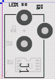
click, Esc. Connect the left LED pin to the bottom header pin.
Connect the right resistor pin to the right LED pin.
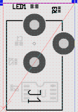
Next we’ll make some adjustments to our PCB. Unless you have your own library that you’ve tweaked to be “just right”, it’s likely that you’ll need to adjust some things during the board layout process. For example, you might need to make room for a trace between two pins. In our case, we’re going to make some adjustments that are appropriate for home-made boards. We’re going to make the pads bigger, in case we drill off-center. There is a generic “change size” command that’s tied to the S key. Place the crosshair over one of the pins and type S and the pin gets bigger. Press Shift-S and the pin gets smaller. You can change the size of pins, pads, traces, and even silk this way. However, if you want to change a lot of things at once, there’s a simpler way. Use the Select→Select all visible objects menu entry to select everything. Now you can use the Select→Change size of selected objects menu to change all the selected things at once. In our case, we want the Pins +10 mil option to make our pins a little bigger. After clicking that, see that all the pins are a little bigger. Now you can Select→Unselect all objects to unselect them all.
You can also use the Select tool (SEL) to select and deselect. To select, either click with the left mouse button on the object you want to select, or drag a rectangle around a group of things. To deselect, just click somewhere where there isn’t anything. You can also Shift-click to select something without deselecting anything else, like if you wanted to select two or three things that aren’t grouped nicely.
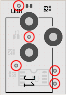
Next we will label our components. Each element has three text strings it can display; you choose which through a View menu option. The default is to display the reference designator (refdes), which is what we want for now.
Since both pins and elements can have labels, turn off the grid so we
can select the elements (View→Grid size→No Grid). Now
select the Edit→Edit name of→text on layout menu. Most of
the GUI goes “grey” and pcb asks you to Select an Object.
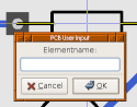
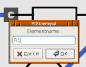
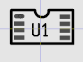
Left-click on the resistor (on the body, not on the pins). A dialog
box pops up asking you for the new name. Make sure it says
“Element” and not “Pin”, and type in R1:
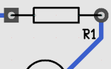
You can now drag and drop the name to where you want it, being careful to pick up the label and not any traces:
You can also use keyboard shortcuts. Position the crosshair over the
LED, but not over the pins, and press the n key (for “name”).
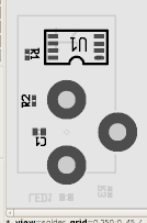
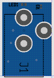
Type in D1. Set the name of the header to J1 and arrange
the names so they look like this:
Don’t forget to save your work occasionally. pcb will normally
save a copy automatically every once in a while, but it’s a good habit
to save it manually when you’re at a good stopping point.
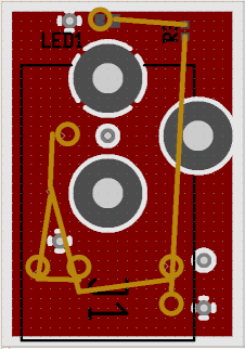
We can also add additional text to the silkscreen and copper layers. Let’s add some text to the header, so we know which way to plug the battery in. We want to use the text tool:
We also want the silkscreen layer to be the default drawing layer:

Now, click below the header’s square pin, and enter + in the
dialog that pops up. Use the S key a whole bunch of times to
make it bigger, then use the selection tool to move it in place. Do
the same for the - label.


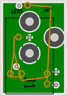
Now that we’re done with the labels, set the grid back to 100 mil in case you move any of the traces or parts; once they’re off-grid it’s hard to get them back on to the grid.
We’re done editing the board now, so if you haven’t already, save your work. But now that the board is done, what do we do with it? Well, that depends on how you’re going to make your board. If you want to do it yourself, you probably want to send it to your printer. If you want someone else to make it, they’ll probably want gerber files.
In your File menu, there are three options we’re interested in.
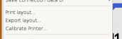
The Print Layout... option prints your layout, but note that it will print 11 pages of board layers! This probably isn’t what you normally want, but let’s do it anyway.
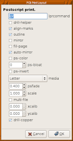
There are a lot of options there, but there’s only a couple you need to worry about right now. Select “fill-page” and “ps-color” and click OK. “Fill-page” zooms your prints to fill the page. “PS-color” causes each layer to be printed in the same color as you see on the screen. If you’re making boards at home using toner transfer, you want these options off, and you want “mirror” on.
In most cases, you don’t want to just print the whole design. Usually you’ll use the Export Layout... option to export your layout in a format that others can use. When you export, a list of possible export types is offered:
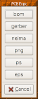
Click on gerber so we can create some Gerber (RS-274X) files, which are industry standard file for describing circuit boards.
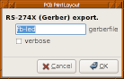
Click on verbose then OK. You’ll see something like this in your terminal:
Gerber: 5 apertures in fb-led.front.gbr
Gerber: 5 apertures in fb-led.back.gbr
Gerber: 3 apertures in fb-led.frontmask.gbr
Gerber: 3 apertures in fb-led.backmask.gbr
Gerber: 2 apertures in fb-led.plated-drill.cnc
Gerber: 3 apertures in fb-led.frontsilk.gbr
Gerber: 3 apertures in fb-led.fab.gbr
For a single sided board, most fab houses will need the back,
backmask, plated-drill, frontsilk, and fab files. pcb always
produces “positive” gerbers in case the fab asks.
For home fabrication, you’ll want to print (see above) without the ps-color or fill-page options. For this simple board, printer calibration is not needed. If you’re drilling your own holes, you may want to select the drill helper option, which reduces the diameter of the holes in the copper wherever you’re drilling to help you center the drill properly. If you use the ps exporter, selecting the “multi-file” option puts each layer in a separate file. That way, you can print only the layers you’re interested in.
So let’s see what we’ve produced. Exit from pcb with
File→Quit Program and find your terminal again. I use the free
programs gv and gerbv to view my exported files;
gv is GhostScript, but your desktop probably knows what to do
if you double click on a .ps file in your file browser. gerbv
is a gerber file viewer that’s part of gEDA:
$ gerbv fb-led.*.gbr fb-led.*.cnc
That’s it! The next step is to actually make board (or have them made), which is beyond the scope of this tutorial.
Next: SMT Blinker, Previous: LED Board, Up: Your First Board [Contents]
This next board will introduce some additional concepts in pcb
that will help you with more complex board. It is assumed that you’ve
gone through the previous board, and those concepts will not be
re-explained. This board will be another single-sided board, but with
additional components. We will use a schematic to describe the
circuit, create some custom symbols and footprints, and learn to use
the autorouter.
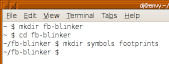
We will begin by creating our custom symbols and footprints. First,
we must create local symbols and footprint directories and teach the
tools to use them. My preference is to create subdirectories in the
project directory called symbols and footprints:
We then create some files to tell gschem and gsch2pcb to
look in these directories. The first is called gafrc and
contains just this one line:
;; (component-library "./symbols")
(component-library ".")
The second is called gschemrc and contains just this one line:
;; (component-library "./symbols")
(component-library ".")
The third is project-specific. The gsch2pcb program can read
its commands from a project file, and we will use this to tell it
about the footprints directory. The file is called
fb-blinker.prj and contains:
elements-dir ./footprints
schematics fb-blinker-sch.sch
output-name fb-blinker
This project file tells gsch2pcb where to get element
descriptions, which schematics to read (we only have one), and what
base name to use for the various output files.
We must create two custom symbols for this project. The first is for
our power jack, and is a purely custom symbol. Creating such symbols
is beyond the scope of this tutorial. Please refer to the
gschem documentation for that. The second symbol uses the
djboxsym utility which you can download from the web (see
http://www.gedasymbols.org/user/dj_delorie/tools/djboxsym.html).
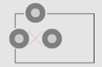
The first symbol is called symbols/powerjack.sym and looks like
this:

There’s a copy of this symbol in the source distribution for this
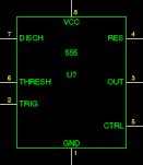
documentation. The second symbol is built from this 555.symdef
file:
[labels]
555
refdes=U?

[left]
7 DISCH

6 THRESH
2 TRIG

[right]
4 RES

3 OUT

5 CTRL

[top]
8 VCC

[bottom]

1 GND
and looks like this:
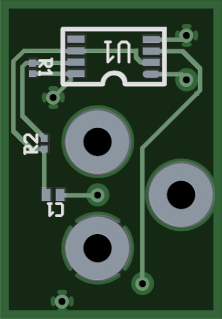
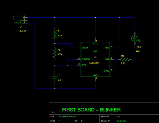
Now, using those symbols, create your schematic, and name it fb-blinker-sch.sch. There’s a copy of the schematic file in the source distribution also. It should look like this:
Using gschem and/or gattrib, set the footprint
and value attributes as follows:
| refdes | footprint | value | |
| C1 | RCY100 | 1uF | |
| J1 | pj102.fp | PJ102 | |
| LED1 | RCY100 | RED | |
| R1 | ACY400 | 100k | |
| R2 | ACY400 | 100k | |
| R3 | ACY400 | 3.3k | |
| U1 | DIP8 | LM555CN |
Now we must create the custom footprint for the power jack. While
there are various contributed tools that can be used for large
footprints (like BGAs), for small parts like this the easiest way is
to create the footprint in pcb itself. This is done by
creating a “board” with vias and lines, then converting it to an
element and saving it.
Change to the footprints subdirectory and start pcb. It
doesn’t matter how big the working area is, or the layer stackup.
Looking at the specs for our power jack, we note that measurements are
given in tenths of a millimeter, so we’ll use a metric grid. To
start, set the grid to 1mm, move the crosshairs to the center of
the board, and press Ctrl-M to set the mark. This will be the
reference point for all our measurements. By doing this with a large
grid value, we ensure that it will be easy to click on the same spot
later on if needed.
Now set the grid to 0.1mm, which we’ll use to place all our vias and lines. We’re using vias to create pins, so we need to set the via size and drill diameter. Click on the Route Style button to bring up the route styles dialog, and set Via hole to 1.6mm and Via size to 3.6mm. While we’re here, set Line width to 0.15mm, we’ll need that when we draw the outline later.
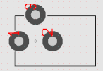
Now, zoom in enough to see the grid points. Place one via 3mm to the left of the mark, one 3mm to the right, and one 4.7mm above. Sequence is important! The pins will be numbered in the same order as the via creation. To place a via, select the Via tool, position the crosshair, and press the left mouse button.


Using the line tool, the same tool you used to draw copper traces in the first board, we will draw an outline of the jack on the silk layer. Select the line tool, and make the silk layer active. Draw as much of a box as you can which extends 10.7mm to the right of the mark, 3.7mm to the left, and 4.5mm above and below. Be careful not to draw on top of your pins, or your board will have ink on the pins. It should look something like this:
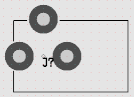
Now, set the grid back to 1mm so we can easily click on the mark. Select everything by using the Select→Select all visible objects menu button. Position the crosshair on the mark and press Ctrl-C to copy all the objects to the buffer. Use the Buffer→Convert buffer to element menu button to convert the buffer to an element. You can now click somewhere else on the board to paste a copy of your new element for inspection.
The first thing to do is check the pin numbers. Place the crosshair on the mark and press the D key to turn on the pin numbers. Check to make sure they’re correct, then press D to turn them back off again.
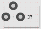
Now, we’re going to set the default position of the label. Place the
crosshair on the mark and press the N key. Change the element
name to J?. By default it shows up at the element’s mark. Use
the selection tool and S key to position the label as shown
below.
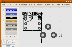
Using the selection tool, position the crosshair on the element’s mark
and click on it to select it. Press Ctrl-C to copy it to the
buffer, and use Buffer→Save buffer elements to file to save your
new footprint to a file. Save it as pj102.fp in the
footprints directory. Note that the name of the file must match the
footprint attribute you used for the power jack in your schematics.
Congratulations! You’ve created your first custom footprint.
Now that we have our schematics and custom footprint, we need to
figure out how to start the board layout. The tool we will use is
gsch2pcb, which reads schematics and can create or update a
board to match. Since gsch2pcb doesn’t use the same defaults
as pcb, we will create the board in pcb and only use
gsch2pcb in update mode.
When creating a non-trivial board, it’s a good idea to start with a
larger board than your final size. For this project, the final size
will be 1.4 inches wide by 0.9 inches high. However, we’ll start with
2 by 2 inch board to give us some room to move things around. Run
pcb and create your board, setting up the size, layers, and
styles just like in the last project. Make sure you set a 100 mil
grid, since the parts we’re using are all designed with 100 mil
spacing in mind. Also, make sure Settings→Crosshair snaps to
pins and pads is checked. Save this empty board as
fb-blinker.pcb and exit.
Now we run gsch2pcb, passing it the name of the project file:
$ gsch2pcb fb-blinker.prj

---------------------------------
gEDA/gnetlist pcbpins Backend
This backend is EXPERIMENTAL
Use at your own risk!
---------------------------------

Using the m4 processor for pcb footprints

----------------------------------
Done processing.  Work performed:
1 file elements and 6 m4 elements added to fb-blinker.new.pcb.

Next steps:
1.  Run pcb on your file fb-blinker.pcb.
2.  From within PCB, select "File -> Load layout data to paste buffer"
    and select fb-blinker.new.pcb to load the new footprints into your existing layout.
3.  From within PCB, select "File -> Load netlist file" and select
    fb-blinker.net to load the updated netlist.

4.  From within PCB, enter

           :ExecuteFile(fb-blinker.cmd)

    to update the pin names of all footprints.
What gsch2pcb does is remove elements from your board that don’t exist in the schematic, provide new elements that need to be added, generate an updated netlist, and create a script that renames all the pins. You don’t need to use all these - for example, I rarely use the pin renaming script - but we will this time, so you can learn how each file is used.
We will do as the hints above tell us to do. Run pcb
fb-blinker.pcb to bring up the empty board. Load the new element
data, which automatically changes you to the buffer tool. Click on
the board to place all those new parts. They’ll all be in the same
place, but we’ll fix that later. Load the new netlist, and run the
script. After closing any dialogs that may have come up, your board
should look like this:
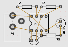
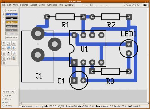
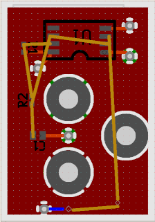
The next step is to separate the elements so we can start laying out our board. Use the Select→Disperse all elements menu option, which spreads apart the elements. Then, use the Connect→Optimize rats nest menu option (or the O key) to draw all the rats on the board. These will help you figure out an optimum layout of your elements. Your board should look something like this (yours may vary depending on how the dispersal worked):
If you position the crosshair over U1 and press the D key, you’ll see that the pins are now labelled with the same labels as in the schematic. You can use the View→Enable Pinout shows number menu checkbox to toggle between the symbolic labels and the original pin numbers.

Now, as before, we want to rearrange the elements to minimise and
simplify the connections. This is where the rats come in handy. As
you rearrange the elements, the rats follow, so you can see how
rotating and moving elements affect the layout. As you move elements
around, press the O key to tell pcb to figure out the
best way of connecting everything in their new locations.
As you move the elements around, remember to pick up the power jack by its mark, as the power jack’s pins have metric spacing. The other elements should be picked up by their pins, since they have inch spacing. By picking up elements by their pins, you ensure that their pins end up on the grid points when you put them down.
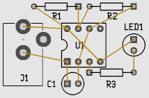
Rearrange your elements so that they look like this, somewhere near the center of your board. Note that the rats nest will tell you when you have the resistors backwards, since they don’t have “polarity” like the LED or IC have.
As before, we want to move the refdes labels around so that they’re both visible and out of the way. To make this easier, use the Settings→Only Names option to keep the tools from accidentally selecting elements or rat lines. Shut off the grid, and use the selection and rotate tools, and the S size key, to make the labels like this:
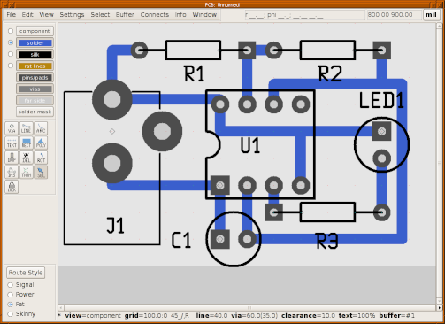
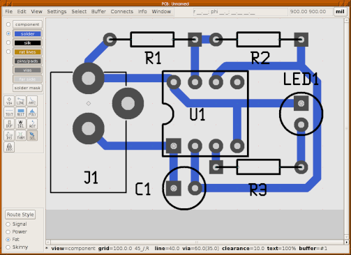
Now use Settings→Lock Names to keep from accidentally moving our labels later. We’re still using our over-sized board. Now is the time to reduce it to the final size. First, we have to move the elements to the upper left corner of the board. Set the grid back to 100 mil, Select→Select all visible objects, grab one of the pins, and move everything up to the corner, as close as you can get without touching the edges:
Click to de-select and change the board size to 1400 mils wide by 900 mils high. Don’t forget to save often!
Again, we’re planning on hand-soldering this board, so select everything and make all the pins 10 mils bigger than the default.
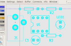
Rather than route all the traces by hand, for this board we will use the autorouter. There are a few key things you need to keep in mind when using the autorouter. First, the autorouter will use all available layers, so we must disable the layers we don’t want it to route on. To do this, click on the component button to disable that layer:

The autorouter also uses whatever the default style is, so select the Fat style:

The autorouter uses the rats nest to determine what connections will be autorouted, so press O now to make sure all the rats are present and reflect the latest position of the elements. To do the autorouting, simply select the Connects→Autoroute all rats menu option.
In theory, you could consider your board “done” now, but to make it look more professional, we will do two more steps. Use the Connects→Optimize routed tracks→Auto-Optimize menu option twice (or until no further changes happen) to clean up the traces left by the autorouter:
And finally, select Connects→Optimize routed tracks→Miter to miter the sharp corners:
Your board is done. As before, you can print your design or produce Gerber files, according to how you’re going to have your board made.
Previous: Blinker Board, Up: Your First Board [Contents]
The third and final board in the “first board” series will teach you about multi-layer boards, vias, and SMT components. Again, we assume you’ve done the other two boards, and will not re-explain concepts taught there. We will be using the same circuit as the last board, but to make things interesting, we will be adding some constraints. The board must be as small as possible, EMI-proof, and able to handle rework. Ok, I’m making this up, but what it means is that we will be using the smallest components a hobbyist can expect to use, a four-layer board, and more vias than would otherwise be needed. We do this to give us the opportunity to learn these techniques, without spending undue time due to an overly large schematic.
We begin with the same schematic as before. To assist us in assigning
power planes, we need to name the power rails in the schematic. See
the gschem documentation for details, but what you want is to
name the ground net GND and the power net Vdd. Set up a
new fb-smt.prj project file as before. Use gattrib to
set the footprint attributes as follows:
| refdes | footprint | value | |
| C1 | 0402 | 1uF | |
| J1 | pj102.fp | PJ102 | |
| LED1 | 0402 | RED | |
| R1 | 0201 | 100k | |
| R2 | 0201 | 100k | |
| R3 | 0201 | 3.3k | |
| U1 | MSOP8 | LMC555CMM |
Run pcb and set up your blank board. Put “component” and
“component side” in group 1. Put “GND” in group 2, “power” in
group 3, and “solder” and “solder side” in group 4. Switch to the
Change tab, select the solder layer in the main window, and
move the solder layer down under the power layer.
Set the board size to 50 mm by 50 mm. To set a metric size, use the
View→Grid units→mm menu option. Then, the Sizes
preference will use millimeters. Set the DRC values to 0.35 mm (about
13.5 mil) for drill and 0.15mm (about 6 mil) for everything else.
Save your board, exit pcb, and run gsch2pcb fb-smt.prj.
Go back to pcb, import and disperse the new elements, and load
the netlist.
As before, move the labels out of the way and size them accordingly. You should end up with something like this:
The final size of our board will be 12.5mm wide by 18 mm high, not much bigger than the power jack. Start by rotating the power jack to face down, and put its mark at 5.5mm by 7mm. The LED goes just above it, with R3 to the right of the LED. The rest of the elements will go on the other side of the board. Here’s how:
For each element that needs to go on the other side of the board, place the crosshair over the element and press the B key
The element shows as a light gray because it’s now on the “far side” of the board (Note that one of the layer buttons says far side on it). You can flip the board over (making the far side the near side, and visa-versa) by pressing the Tab key. Since the elements we need to place are on the far side, now, flip the board over. Note that this is an up-down flip, so the power jack now appears in the lower left corner instead of the upper left. There are other types of flips you can do by using Shift-Tab (left-right flip), Ctrl-Tab (180 degree rotation), or Ctrl-Shift-Tab (nothing moves, sort of an X-Ray view).
Anyway, move the remaining elements around so that they look like this:
When routing a multi-layer board, I find it best to start with the
power and ground planes. First, resize the board to be 12.5 mm wide
by 18 mm high, and flip it so you’ve viewing the component side (the
side with the power jack). If your version of pcb does not
permit sizes this small (some versions have a one inch minimum, others
0.6 inch), save the file, exit pcb, and edit fb-smt.pcb
in a text editor so that the PCB line looks like this:
PCB["" 49213 70866]
When you run pcb again, the board will have the right size.
Set your grid to 0.5 mm and make sure it’s visible. There are two
ways to create a “plane layer”, which means a layer that’s mostly
copper. Such layers are often used for power and ground planes. The
first way is to use the polygon tool; the second is to use the
rectangle tool, which is just a shortcut for the polygon tool.
Make the GND layer the current layer and select the POLY tool:
The polygon tool works by clicking on each corner of the polygon, in sequence. You complete the polygon by either clicking on your start point again, or by pressing Shift-P. We will create a polygon that’s 0.5mm away from the board edge. In these images, we start at the lower left corner and work our way around clockwise. When we click on the lower left corner again, the polygon is created:
In this case, we’re just drawing a rectangle, but if you need any other shape, just click on the corners as needed. As a shortcut, you can create a rectangle with the rectangle tool, which creates rectangle-shaped polygons. Make the power layer the current layer and select the RECT tool:
Like the polygon tool, the rectangle tool works by clicking on corners. However, you only have to click on two diagonally opposite corners, like this:
If the color difference is too subtle for you, you can choose other colors through the File→Preferences menu option. We will set the GND layer to green and the power layer to red for the remainder of this tutorial.
To connect the ground and power planes to their respective nets, we’ll use a thermal to connect the power jack’s pins to them. We could also just draw a line from the pin to the polygon, but thermals are better suited to this task. Select the THRM tool:
What the thermal tool does is connect (or disconnect) thermal fingers between pins or vias, and the polygons around them. Each time you click on a pin or via, the thermal fingers are connected to the current layer. We want to find the pin on the power jack that’s connected to ground in the schematic, and connect it to ground on the board. We use the netlist dialog to do so. First, optimize the rats net with O and make the GND layer current. If the netlist dialog isn’t shown, use Window→Netlist to show it. Select the GND net and click on Find:
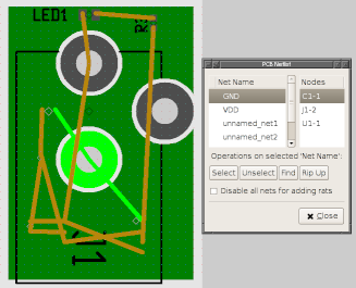
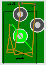
Notice that one of the pins on the power jack has been highlighted. That’s the one that is supposed to be connected to the ground plane. Click on it to create a thermal:
If you optimize the rats nest again, the rats won’t connect to that pin any more, and the other pins and pads that need to connect to the ground plane are now marked with circles, meaning “these need to be connected to a plane”. Anyway, make the power plane the current plane, find the VDD net in the netlist and create its thermal on the found power jack pin. Note that the green GND thermal fingers on the other pin show through the gap in the red power plane - thermals are created on a specific layer, not on all layers.
If you tried to autoroute the board at this point, it would just connect all those power and ground pins to the power and ground pins on the power jack. So, we will first tie all the power and ground pins to their planes manually, using vias. We’re doing this mostly to demonstrate how to do it, of course. The first step is to place the vias. Select the VIA tool from the left panel:

Click on the Route Style button to bring up the route styles dialog, and set Via hole to 0.4mm and Via size to 0.8mm. Also set Line width to 0.25mm. Create vias near the pins that are connected to the planes, as such:
Note that I’ve shut off the ground and power planes, as well as rat lines, to help you see where the vias should go. Shut off the GND plane and “find” the VDD net again, to highlight which rat circles (and thus their vias) need to connect to the power plane. Like you did with the power jack’s pins, use the thermal tool to connect the relevent vias to the power plane. Repeat for the GND plane.
Now you have to connect the vias to the pins that need them. For the LED it’s easy, that trace goes on the top. Make the component layer the current layer and use the LINE tool like you’ve done before to draw a line from the via next to the LED, to the pad on the LED that’s connected to VDD. For the other connections, you’ll want to flip the board over, so use the Tab key to flip the board over, make the solder layer the current layer, and connect the rest of the power/gnd pins to their vias. If you press O now, you’ll see that all the rat-circles have gone away:
The last step is autorouting. Hide all the power, ground, and silk layers, optimize the rats nest (O), and run the autorouter, optimizer, and miterer. Done! Here’s what the board looks like with the “thin draw polygons” setting checked, to only draw outlines for the power and ground planes, along with some photo-quality prints: